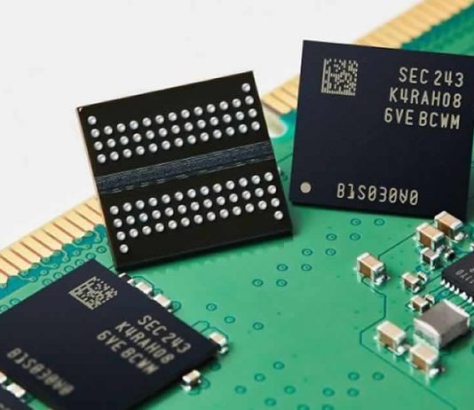
Samsung has officially announced the commencement of mass production for DDR5 DRAM chips using its latest 12nm manufacturing process. This technological breakthrough allows Samsung to enhance the efficiency and performance of its DRAM devices while reducing costs compared to previous generation nodes.
The new DDR5 memory chips, featuring a capacity of 16 gigabits, are manufactured using Samsung’s industry-leading 12nm class process technology. While Samsung had previously produced 16Gbit DDR5 chips, the adoption of the newer and smaller 12nm process delivers notable advantages in terms of power consumption and die size. In comparison to DDR5 dies manufactured on the company’s previous-generation 14nm node, the 12nm dies exhibit up to 23% lower power consumption and enable the production of 20% more dies per wafer, according to Samsung.
A significant innovation in the 12nm DRAM manufacturing process is the utilization of a new high-k material for the capacitors in the DRAM cells. This advancement allows for improved static electricity within the cells, enhancing performance without increasing the dimensions or size of the die. Higher capacitance in a DRAM cell translates to increased data storage capacity and reduced power-consuming refresh cycles, thereby boosting overall performance. Samsung’s achievement of shrinking the die size is particularly noteworthy since analogue components like capacitors face limitations in further size reduction as process nodes shrink.
Samsung’s 12nm DDR5 ICs not only introduce new high-k materials but also feature reduced operating voltage and noise, offering an optimized balance between performance and power consumption compared to their predecessors.
Another remarkable aspect of Samsung’s 12nm DRAM technology is that it appears to be the third generation production node employing extreme ultraviolet (EUV) lithography. The initial D1x node served as a proof of concept, while its successor, the D1a, has been in use since 2021, utilizing EUV for five layers.
Moreover, Samsung’s new 12nm DDR5 die exhibits the potential for faster memory speeds, capable of reaching DDR5-7200 (or 7.2 gigabits per second per pin). This speed surpasses the current official JEDEC specification, opening possibilities for future XMP/EXPO memory kits. Although the required voltage has not been specified, this development instills hope for further advancements in memory technology.
