

Tesla is building the world’s most powerful supercomputer, called Dojo — which is supposed to deliver more performance with less consumption and less space. Dojo should achieve over 1 ExaFLOPS.
After Tesla has already designed the hardware for its electric cars with the FSD (Full Self Driving) chip, the D1 processor is the counterpart for the Dojo supercomputer. Tesla combines thousands of these chips, and the first racks are due to be installed soon.
For the training of artificial neural networks, Tesla currently relies on three clusters that work with a total of 11,544 Nvidia GPUs. A smaller cluster with 1,752 GPUs, 5 PB NVMe storage and InfiniBand adapters for networking the components is used for automated labeling, while two larger clusters, one with 4,032 GPUs and 8 PB NVMe storage and one with 5,760 GPUs and 12 PB NVMe storage, for the training with a total of 9,792 GPUs are responsible.
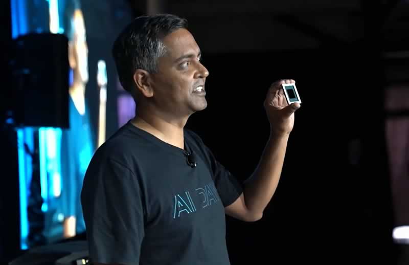
With “Project Dojo”, Tesla wants to build its own supercomputer architecture. Ganesh Venkataramanan is responsible for Project Dojo, who explained the structure of the processor and the supercomputer at Tesla AI Day.
The centerpiece is the specially developed D1 chip with 50 billion transistors from 7 nm production on an area of 645 mm². The processor provides a computing power of 362 TFLOPS based on BF16 and CFP8 (Configurable Floating Point 8) and 22.6 TFLOPS for FP32. Tesla specifies the TDP of the chip with 400 watts.
A D1 consists of 354 training nodes, each of which is home to a 64-bit superscalar CPU with four cores, which is specially designed for 8 × 8 matrix multiplication and the formats FP32, BFP16, CFP8, INT32, INT16 and INT8. Training nodes have a modular structure and, according to Tesla, can be linked in all directions via a “low latency switch fabric” with an on-chip bandwidth of 10 TB/s. Tesla spans an I/O ring around the D1 with 576 lanes of 112 Gbit/s each for an off-chip bandwidth of 4 TB/s per side.
The total of 1,500 D1 chips are not directly linked to one another, but are combined in 5 × 5 units on a so-called training tile. Training Tile is then also the unit of measurement that Tesla uses for the entire Dojo supercomputer. 25 D1 dies are combined in a fan-out wafer process to form a training tile, which in turn has its own I/O ring with 9 TB/s in four directions and thus a bandwidth of 36 TB/s has.
Tesla calls the Training Tile the largest “organic multi-chip module” currently in the industry. For the design, Tesla had to develop completely new tools that did not exist before. A training tile of 25 D1 delivers 9 PetaFLOPS BF16 or CFP8.
The energy is supplied vertically via a self-developed voltage regulator module that is applied directly to the fan-out wafer. In addition to the electronic structure with a 52 volt DC power supply, Tesla also independently developed the entire mechanical structure, including cooling. The latter must be able to dissipate waste heat of at least 25 × 400 watts only for D1, but including the other components, the solution is designed for 15 kilowatts.
The finished module has a volume of less than a cubic foot, explains Tesla, which corresponds to around 28 liters. Last week Tesla put the first functional training Tile into operation at a clock rate of 2 GHz with limited cooling on a bench table for test purposes.
Tesla, in turn, combines the training tiles in trays of 2 × 3 tiles and two of them in a cabinet, so that more than 100 PetaFLOPS are available per server cabinet with a bidirectional bandwidth of 12 TB/s. The end product is the finished Dojo supercomputer “ExaPOD” with 120 training tiles distributed over 10 cabinets and a total of 3,000 D1 chips, which in turn have a total of 1,062,000 nodes. Tesla gives the total computing power with 1.1 ExaFLOPS for BF16/CFP8.
Upon completion it will stand for the world’s fastest AI training supercomputer with four times the performance, 30 percent higher performance per watt and five times smaller footprint — at the same costs as before with Nvidia.