

AMD has recently revealed some details about the “Instinct MI300”, a next-generation data centre APU currently under development.
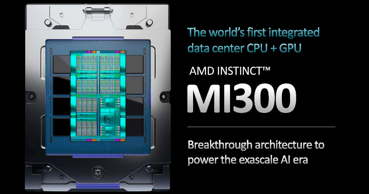
CEO Lisa Su held the silicon chip in her hand and provided some basic specifications, reiterating AMD’s desire to lead the HPC market. It utilizes multiple chiplets fabricated on TSMC’s 5nm process, stacked on top of each other and connected with on-package HBM memory, which is intended to maximize available memory bandwidth.
The Instinct MI300 is a massive 146 billion transistor chip, the largest and most complex AMD has ever built. This is significantly more than the 100 billion transistors Xeon Max GPU from Intel or the 80 billion transistor GH100 GPU from NVIDIA. The MI300 will feature 24 AMD Zen 4 CPU cores and an as-yet-unannounced CDNA 3 architecture GPU with 128GB of HBM3 memory. It will be built with nine 5nm chiplets and four 6nm chiplets, with the 5nm chiplets likely being Compute Logic chipsets (i.e. CPU and GPU chiplets). The MI300 is expected to offer improved AI performance per watt and AI training performance compared to the MI250X.
One of the key advantages of the Instinct MI300 is its ability to share a high-speed, low-latency unified memory space between the CPU and GPU cores. This enables fast and easy data transfer between the two and allows each to perform the types of computing at which they excel.
In addition to its impressive technical specifications, the MI300 also represents a significant shift in AMD’s strategy for the data centre market. The company has traditionally relied on a combination of its EPYC CPUs and discrete MI250X GPUs for its HPC offerings. The MI300 marks the first time AMD has attempted to bring these two components together in a single package. This should simplify operations for customers, as they will no longer have to manage two separate components and deal with the challenges of connecting them through MCM wiring.
Using chiplets and 3D die stacking also allows AMD to take advantage of the latest advances in manufacturing technology, resulting in a more efficient and powerful processor. The combination of 5nm and 6nm chiplets should provide the perfect balance of performance and power consumption. At the same time, the on-package HBM memory should enable much higher memory bandwidth than what is currently possible with traditional memory interfaces.
Overall, the MI300 looks to be a very promising offering from AMD and could potentially shake up the data centre market if it can deliver on its performance and efficiency promises. The company’s decision to focus on HPC and AI applications is a smart move, as these areas are expected to see significant growth in the coming years. With the MI300 set to launch in 2023, we should have a better idea of its capabilities soon.