

Intel has made significant progress in developing the Intel 18A (1.8nm-class) and Intel 20A (2nm-class) manufacturing processes. These processes will be used to manufacture chips for Intel’s products and its Intel Foundry Services (IFS) division customers.
Wang Rui, president and chairman of Intel China, announced that the company had finalized the development of these processes. Intel has determined all the specifications, materials, requirements, and performance targets for both technologies. This is a significant milestone in the development of these processes.
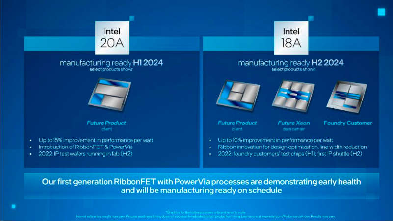
The Intel 20A manufacturing process will use Gate All Around (GAA) RibbonFET transistors and PowerVia backside power delivery (BPD). This process involves shrinking the metal pitch, introducing a new transistor structure, and adding backside power. It is a significant challenge, but it will enable Intel to surpass competitors TSMC and Samsung Foundry, allowing it to regain its former glory. Intel plans to start using the node in the first half of 2024.
Intel 18A manufacturing process further refines the company’s RibbonFET and PowerVia technologies to reduce transistor size. The development of this node is progressing well enough that Intel is pushing its introduction to late 2025 to late 2024. Originally, Intel planned to use the Twinscan EXE scanner with 0.55 numerical aperture (NA) optics, ASML’s High NA, for the 1.8 Angstrom node but decided to start using this technology early, so it decided to use 0.33NA. The company expects that when 1.8nm-class manufacturing technology enters HVM (High Volume Manufacturing) in the second half of 2024, it will become the most advanced node in the industry.